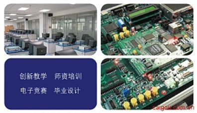
Program description:
The system platform adopts the structure of core board + innovative development experiment platform, integrates commonly used hardware interfaces, and can achieve SOPC, ARM, DSP, core board superposition expansion through the core module expansion interface, fully meets EDA, SOPC, ARM, DSP, single chip Teaching experiment, graduation design, course design, etc.
The system platform supports uc / osII and uClinux embedded operating systems, and supports quartus II version 10.1 design software, including SOPC Builder system development tools, Nios II integrated development environment (IDE) and debugger.
The system platform provides detailed experimental instructions to complete digital logic circuit design experiments, sequential circuit design experiments, memory design experiments, general interface circuit experiments, SOPC hardware system design and software programming design experiments, uc / osII embedded system experiments, UClinux-based CGA network server controls LED, LCD, DA and other uClinux experiments, hardware design IP core application design experiments, DSP innovative technology experiments, etc.
Core board hardware parameters:
â— ALTERA Cyclone â…¢ EP3C55 chip, the equivalent gate number is 3.6 million gates
â— The 4x64 pin core module expansion interface can be seamlessly combined with other SOPC boards, ARM boards, DSP boards, single-chip boards and motherboards, and can also expand memory through expansion ports, which can not only achieve large-capacity storage of data, but also improve data Access speed
â— 2 x16 / 32/64 Mb 16-bit bus FLASH chips
â— 2 x 4 / 8Mb 16-bit bus SRAM
â— 2 x64 / 128Mb 16-bit bus SDRAM
â— IIC EEPROM + special reset chip
â— 1 JTAG interface
â— 1 AS interface
â— 1 configuration circuit: with serial EPCS16 chip or EPCS64 chip
â— 2 USB2.0 ports
â— Power circuit
â— 8 LED user indicators
â— 1 configuration button for reconfiguration
â— One system reset button to generate system reset signal
â— 4 multi-function buttons
â— The core board can be used independently or can be stacked on top of each other
Platform hardware parameters:
â— The motherboard is carefully designed with 6-layer board industrial standards, and undergoes strict EMI and signal integrity system tests to ensure high reliability and high speed of the motherboard
â— 4X64Pin core module expansion interface: SOPC, multi-core MPSOC, 8/16 / 32-bit single-chip microcomputer ... core board superposition
â— IIC EEPROM / reset circuit interface module: board level 3.3V working voltage
â— 1 channel single pulse positive polarity signal output, 1 channel single pulse negative polarity signal output: board level 3.3V working voltage
â— One 8-bit high-speed parallel PAR bus ADC, the speed is 50Msps, 8-bit 75Msps ADC can be selected
â— Two 8-bit high-speed parallel PAR bus DAC, the speed is 125Msps
â— SMBUS bus: digital temperature control sensor circuit interface module
â— Onewire bus: RTC real-time clock interface module
â— 8-channel FPGA external expansion interface module (signal output) I / O multiplexing
â— 8-channel FPGA external expansion interface module (signal input) I / O multiplexing
â— 5 inch IDE standard expansion interface module
â— 2.5 inch / 3.5 inch IDE standard expansion interface module
â— PS connect keyboard / mouse interface module
â— RS232 interface module
â— IRDA infrared communication interface module
â— USB2.0 / UART interface module
â— RS485 interface module
â— VGA interface module
â— Audio power amplifier interface module
â— 1 way speaker interface module
â— 1 channel buzzer interface module
â— 4 phase stepper motor interface module
â— DC motor interface module
â— SD card interface module
â— CF card interface module
â— 4X4 mobile phone keyboard array interface module
â— 2x8 total 16 LED indicator interface modules
â— 10 independent key input interface modules
â— 2x8 total 16-channel switch signal input interface module
â— Four 8x8 dot matrix to form 16x16 dot matrix dynamic scanning interface module
â— 8 interface modules with dynamic scanning of total seven-segment digital tube
â— Board level function module control selection dial switch: support 4/8 bits
â— PLL clock output interface module: support PLL / embedded logic analyzer
◠14 clock sources: 0.5Hz / 1Hz …… 24MHz interface module
â— Mobile phone camera interface module: optional support 1.3 million pixels / 3.2 million pixels
â— The clock source of the mobile phone camera is indeed saved as 12Mhz (optionally with in-line active crystal oscillator)
â— 2 lines x16 character LCD interface module
◠4.3 ″ TFT color touch LCD interface module
â— USB-Blaster download / simulation / debugger can also be used independently
â— 8/16 bit digital memory expansion interface EM2 module: support data bus D0-D15, address bus A0-A22, control bus BnOE, BnWE, LOWER_BYTE, UPPER_BYTED, reset signal, etc., plus 11 I / O user-defined expansion Circuit
â— 24-bit stereo Audio codec interface module: 1 LINE-out, 1 HP-out, 1 MIC-in, 1 LINE-in
â— Independent 50 I / O user-defined expansion board circuits: support 3.3V / 5V (TTL / CMOS level), expansion board power supply supports 12V, 5V, 3.3V
Experimental content:
(A total of 136, only a part is listed below)
* Modern EDA technology experiment:
1. Sequence Generator
2. I2C interface control (with temperature control chip) experiment
3. Design and use of dual-port RAM
3. Stepping motor subdivision control experiment, DC motor experiment
5. VGA image display controller to realize table tennis game
6. Vending machine
7. Electronic combination lock
8. Digital voltmeter
9. Four person answering device
10. Color LCD screen game control experiment
* SOPC technology experiment:
1. Establish Nios II system with parallel data bus Flash and FLASH programming experiment
2. I2C-RTC real-time clock experiment
3. PWM nuclear custom experiment
4. SMBUS bus-temperature acquisition experiment
5. Experiment based on touch screen calculator
6. Drawing experiment of color TFT liquid crystal display
7. 8051 single-chip IP core design
* Modern DSP and communication technology experiment:
1. Design of controllable sine signal generator
2. Design of Digital Frequency Synthesizer (DDS)
3. FSK modulator design
4. IIR digital filter design
5. Design of AM signal generator
6. FM signal generator design
7. Frequency sweep signal generator
8. Application design of FIR digital filter (IP core)
9. Use FFT IP Core in DSP Builder
10. Customize user peripherals based on Avalon bus in DSP Builder
11. Nios instruction customization method based on DSP Builder
The above scheme is configured as:
B-ICE-EDA / SOPC-IEELS host, GX-SOPC-EP3C55-FBGA484 core board, USB-Blaster download debugger, 4.3-inch touch screen, standard accessories, supporting CD-ROM, supporting teaching materials
Convenient folding for long battery life.
Electric scooter
fold
Jiangsu Anywhere Mobility LTD. , https://www.annelectricscooter.com