Foreword
To ensure that the excellent rate of wafer bumping using screen printing is at an ideal level, a number of important design factors must be considered.
Screen Printing
Screen printing technology using standard surface mount equipment is a cost-effective solution for attaching wafer bump pads in a simple and mature process environment. With this approach, different applications require different custom design guidelines and follow specific equipment, materials, and process instructions to establish stable, high-yield wafer bump printing and reflow soldering procedures.
Parameters affecting the good rate
Although screen printing is straightforward, many variables can seriously affect the quality or yield of wafers using such bumping methods. A known wafer die value (KGD) is often used to evaluate a wafer bumping process. Performance. In-depth knowledge and high regard must be given to the many design aspects that affect this process, and effective and reliable design strategies should be developed to achieve superior results.
Flip chip bond pad design
One of the advantages of flip chip over wire bonded, face-up chip-on-board devices is that since the conductive pads can be placed anywhere on the active side of the die, they can be on a smaller integrated circuit area. Increase the number of I/Os. However, the screen printing projections may be the printing method that is most limited and hindered by the die pad layout. The size, shape, and spacing of pads must be carefully designed to achieve the desired solder bump size in real-world conditions; in addition, the pad bond surface combinations commonly referred to as bump bottom metal must be considered. In the reflow process, UBM has a significant impact on the formation of screen printed solder balls, and ultimately will affect the strength, reliability and performance of the assembled flip chip.
Pad size and shape
The size of the pad on the chip has a direct effect on the amount of solder paste required to produce the specified reflow bump size for screen printing. To maintain the specified bump height, the larger pad on the chip requires more solder paste: Less solder pads require less solder paste. If the pad is too small, the solder area for supporting a larger amount of solder paste is smaller, and bumps and solder joint strength are significantly affected, but the benefit is only a slight increase in the gap distance. The shape of the wettable soldered area of ​​the chip pad also affects the bump size of the solder paste. This shape is not necessarily related to the geometry of the pad, but is primarily determined by the passivation opening in the pad (see Figure 1).
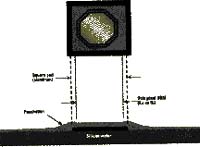
Figure 1: The passivation film opening of the pad determines the solder paste
The size and geometry of the raised wettable bond area.
The shape of the actual bond point in Figure 1 is octagonal, and the pad is square. This shape is defined by the passivation window to reduce the stress concentration on the various corners of the solder ball base. These stress points may weaken the bond strength, and Affect the reliability of solder joints. To reduce this, circular passivation openings are ideal. However, some wafer production systems have problems in manufacturing rounded corners that are opposite to the sharp corners.
One of the experiences is to keep the size of the pad bond point no more than half of the gap, with a minimum of 65 μm (Note 1). To calculate the size of reflow bumps as a function of pad size and geometry, the following equation can be used. This equation simulates reflow bumps, represented by flat, geometric spheres, that can be used as screen design tools to help determine the appropriate screen hole size to apply the required amount of solder paste.
Solder bump projection volume: {1/2 (pad area) x (projection height)} + {1/6Ï€ (projection height) 3}
Pad spacing and location
Whether or not the screen printing can generate large solder bumps on the wafer depends on the pad configuration and density. We suggest that the wider the pitch of the solder pads, the better, so that there is greater flexibility in designing the shape and location of the perforations, thereby maximizing throughput. The high-density layout can also be designed more efficiently to screen printing that allows for larger solder paste coating by simply staggering adjacent pads. Designing a stencil with a multi-row pad configuration is more challenging because the metal foil surface of the stencil will be full of perforations and become very complicated. The current state-of-the-art precision pitch screen printing technology seems to stay at the critical level of 6mil, but these boundaries are constantly being challenged. Although printing can be performed at a smaller pitch, the amount of solder paste that can be applied without flaws is very limited, allowing the industry to set up bump sizes, gaps, underfilling capabilities, solder joint strength, and Attention to issues such as overall reliability.
In terms of pad location, in general, the corner pads on each die are the locations on the wafer where it is most difficult to achieve consistent and flawless printed solder paste volume. The use of non-standard perforated shapes is necessary here because high-density perforations can take up a large amount of screen area, and the unique shape of the perforations makes it difficult to predict the transfer efficiency when coating, so the height distribution of bumps on the bare die may not be People are satisfied. Only by eliminating all corner pads on the wafer can this potential problem be avoided and the perforated design of the stencil can be made more flexible.
Raised bottom metal
In reflow soldering, the printed solder paste must be properly adhered to the wafer pad. The pad metallurgy must be bonded to the solder paste alloy. Most of the die pads are made of aluminum and do not adhere well to eutectic Sn/Pb solder pastes. Therefore, a layer of interstitial material is required to bond aluminum and eutectic Sn/ Pb solder paste, covering the surface of the aluminum pad. After adding a protective passivation film and adding this raised bottom metal layer, there are various options for the available raised bottom metal layer and coating technology. As the cost of the raised bottom metal coating process is high, the industry is competing with each other. Finding economical materials and processes. In this case, the information about the raised bottom metal is proprietary and difficult for the public to access. One of the proven, low-cost, bumped bottom metal methods requires electroless plating, nickel plated aluminum pads, and then immersed in gold. In this process, only the part of the metal that has not been passivated (ie, the aluminum bond pad) will be covered by the nickel/gold bump bottom metal layer. To maintain good wetting characteristics, this raised bottom metal must be as clean and oxidation free as possible. It is best to store the wafers in a nitrogen-controlled insulated storage cabinet to prevent the formation of poor oxidation residues.
Tray design
Since the wafers are very fine objects, shipping is a key issue. In screen printing, plastic or metal trays that are 1.5 inches larger than the wafers should be used to carry the wafers. Larger trays allow the transfer head to have a large enough surface to apply and rotate the solder paste. Permeate completely into the perforation.
Another important factor in designing an appropriate tray is the notch used to hold the wafer. The depth of the notch must allow the upper surface of the wafer to form a plane with the periphery of the tray. The profile of the raised wafer tray is shown in Figure 2.
Figure 2: Wafer raised pallets, vacuum channels under the wafers help to secure the wafers firmly on the tray.
Stencil design
Stencils can be said to be the most important tools. They must be properly designed to achieve high and good rates of outstanding performance. The role of the stencil is to divide the solder paste into a carefully calculated number and place it on the metallurgical bond point on the wafer. It is not easy to successfully create mesh perforation designs that can achieve flawless results, and high reflow bumps are closely spaced, especially if the spacing of multiple rows of die pads is less than 10 um. Projects that affect stencil cutting of wafer bumps include stencil thickness, hole size, shape, orientation and position, and image alignment.