Attack Technology Analysis and Security Design Strategy of RFID Chip
In the past, it was widely believed that IC cards have unmatched security performance due to the use of various sophisticated authentication algorithms, keys, etc. to protect data from unauthorized use. But in the mid-1990s, most of the IC card processors were successfully reverse engineered, so this view has changed a lot. In addition to adopting newer design techniques, it is more important to consider anti-attack measures in the design and implementation of IC card chips to protect important data from being illegally used. The emergence of contactless IC card (RFID) is an important milestone in the development of smart cards: it realizes the non-contact transmission of energy and signals through magnetic coupling or microwave, which effectively solves the problem that the contact smart card uses mechanical electrical contacts. Electrostatic breakdown, mechanical wear, vulnerability to pollution and the impact of humid environments are considered important replacement technologies for identification, bus bills, and logistics. Without the exposed electrical contact nodes, RFID has a certain improvement in security compared with contact IC card products, but it does not change the smart card using authentication algorithms and keys and other security means, so it is not in essence. Solve security issues. It is necessary to learn from the mature experience of contact smart card security design to avoid major technical errors. Smart card attacks generally start with destructive reverse engineering, and their conclusions can be used to develop inexpensive and fast non-destructive attacks, one of the most common and most effective smart card attack modes. b. Memory readout technology Non-destructive attack and its prevention In principle, the power supply of the RFID is integrated inside the AFE and seems to be far from the danger of current analysis, but it is not. Figure 4 shows the schematic diagram of the RFID contact test: By directly loading the AC signal in accordance with the specifications at both ends of the RFID antenna and the series divider resistor, the RFID load feedback signal can be superimposed on the loaded signal directly in the wireless mode. On the AC signal. Since the power consumption variation of the chip is essentially the same as the load modulation, if the power supply design of the AFE is not appropriate, the state in which the RFID micro-processing performs different internal processing may be reflected on the AC signals at both ends of the series resistor. Flat Washers,Washers,Spring Washers ,Non-Standard Nuts XINXING FASTENERS MANUFACTURE CO.,LTD , https://www.hex-bolts.com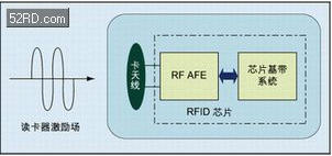
Figure 1: RFID chip structure and working mode
Structurally, RFID is a monolithic integrated circuit that includes both the RF analog front end (RF AFE) and baseband signal processing (see Figure 1). The baseband system includes control logic (or even a microprocessor) and the necessary memory. The AFE part is the energy and signal interface of the RFID. It provides auxiliary signals such as power and clock required for the operation of the on-chip baseband system to complete the data receiving and transmitting functions. Because the RF AFE shields the power supply, clock, power-on reset (POR) and other signals on the smart card from the outside world, it reduces the point of attack implementation to a certain extent, and has a certain improvement in security compared with the contact smart card. .
Smart card chip attack technology and countermeasures
According to whether the physical packaging of the smart card chip is destroyed, the attack technology of the smart card can be divided into two categories: destructive attack and non-destructive attack.
Destructive attack and chip reverse engineering were consistent in the initial steps: removing fumes from the die with fuming nitric acid; cleaning with acetone/deionized water/isopropanol; further removal with hydrofluoric acid ultrasonic bath The metal of each layer of the chip. After the chip package is removed, the electrical connection of the chip function pads to the outside world is restored by gold wire bonding, and finally the manual micro-probe can be used to acquire the signal of interest. For deep sub-micron CMOS products, there are usually more than three layers of metal wiring. In order to understand the internal structure of the chip, it may be necessary to remove the information required to reconstruct the chip layout design. Based on understanding the internal signal traces, the focused ion beam (FIB) repair technique can even be used to connect the signal of interest to the surface of the chip for further observation.
Non-destructive attacks are mainly targeted at products with microprocessors, which mainly include software attacks, eavesdropping techniques, and fault generation technologies. Software attacks use the general communication interface of the microprocessor to seek security protocols, encryption algorithms and their physical implementation weaknesses; eavesdropping technology uses high time domain accuracy methods to analyze the various electromagnetics generated by the power interface during normal operation of the microprocessor. Simulation characteristics of radiation; fault generation techniques allow the processor to generate faults by generating abnormal application environmental conditions, thereby obtaining additional access paths. 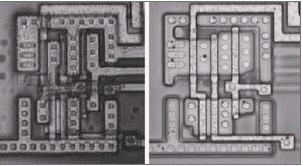
Figure 2: Optical photo of an inverter driven by a NAND gate (containing a metal layer and removing the metal layer).
Destructive attack and its prevention
a. Layout reconstruction
An important step in a destructive attack is to reconstruct the layout of the target chip. By studying the connection mode and tracking metal connections across the boundaries of visible modules (such as ROM, RAM, EEPROM, ALU, instruction decoder, etc.), some basic structures on the chip, such as data lines and address lines, can be quickly identified.
The photo on the surface of the chip only shows the connection of the top metal completely, and it is opaque. With the high-performance imaging system, the lower layer information can be identified from the top unevenness, but for the CMOS process that provides the oxide layer flattening, the metal needs to be removed layer by layer to further understand the various structures underneath. Therefore, a CMOS process that provides an oxide layer flattening is more suitable for smart card processing including RFID.
Figure 2 is an optical layout photo of a NAND gate driving an inverter, similar to the different layers of the figure for the experienced person is no different from the circuit diagram.
For RFID design, the RF analog front end needs to be implemented in a fully customized way, but the HDL language description is often used to implement complex control logic including the authentication algorithm. Obviously, the implementation method using the standard cell library synthesis will speed up the design process. But it also provides great convenience for reverse engineering-based destructive attacks. This standard cell library-based design can automatically implement layout refactoring using a computer. Therefore, the use of a fully customized method to achieve RFID chip layout will increase the difficulty of layout reconstruction to a certain extent.
The technique of layout refactoring can also be used to obtain the content of a read-only ROM. The bit pattern of the ROM is stored in the diffusion layer, and after removing the cover layers of the chip with hydrofluoric acid (HF), the contents of the ROM are easily recognized according to the edge of the diffusion layer (Fig. 3).
In a microprocessor-based RFID design, the ROM may not contain any encrypted key information, but it does contain enough I/O, access control, encryption programs, etc., which are especially important in non-destructive attacks. Therefore, for RFID designs using microprocessors, it is recommended to use non-volatile memory storage programs such as FLASH or EEPROM. 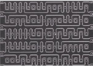
Figure 3: Photo of a NOR-type ROM with metal and POLY connections removed.
For non-volatile memories that store important content such as keys and user data, they cannot obtain information from them through simple optical photographs. During the secure authentication process, at least these data areas are accessed once, so the micro-probe can be used to listen to signals on the bus to obtain important data. For good design, simple repetitive authentication is not enough to access all of the critical locations of the memory. For example, using different encryption keys and encryption algorithms in the same card, and then switching between them every few weeks, the chip's algorithm and key storage area cannot be processed by the processor until it is activated by the broadcast call. Control and so on, making it difficult for early passive monitoring buses to discover these secrets. These experiences with contact smart card ICs can be applied to RFID designs.
Some documents mention that in order to ensure the integrity of the memory data, it is necessary to calculate and verify the verification result of the memory after each chip reset. In fact, this method provides a means for the attack to quickly access all the memory.
In the use of RFID with microprocessors, it is also necessary to consider the security issues caused by software designers' abuse of CPU components (such as address counters) to improve code efficiency. The program counter is automatically incremented every instruction cycle. If it is used for the address generator of memory read and write, the attack only needs to prevent the processor from executing instructions such as JUMP, CALL and RETURN to disturb the normal read order. That is to say, some laser connections are cut off slightly, and the instruction decoder and the program counter circuit can be modified to achieve full access to the memory.
The top-level detector grid is one of the most effective means to prevent micro-probes from acquiring memory data. It makes full use of the multi-layer metal provided by deep sub-micron CMOS technology, and the detector grid can be continuously monitored on the top of important signal lines to continuously monitor short-circuit and open circuit. . When powered, it prevents laser cutting or selective etching to capture the contents of the bus. Based on the detector output, the chip can immediately trigger the circuit to clear all of the contents of the non-volatile memory. These meshes also have an effect on the reconstruction of the metal layers underneath them, because the etching is not uniform, and the pattern of the upper metal is visible in the lower layer, which causes a lot of trouble for the automatic reconstruction of the layout. Manual probes typically have a target size of around 1 micron, and probe stations with tips less than 0.1 micron are priced at hundreds of thousands of dollars and are extremely difficult to obtain. A well-designed grid will make manual microprobe attacks difficult to implement, and general FIB patching techniques are difficult to overcome. 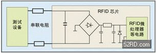
Figure 4: RFID contact method test principle
Non-destructive attacks are primarily for products with microprocessors. A microprocessor is essentially a collection of hundreds of flip-flops, registers, latches, and SRAM cells that define the current state of the processor and, in combination with combinatorial logic, know the state of the next clock. The analog effects of many similar systems can be used for non-intrusive attacks, where:
1. Each transistor and connection has resistance and capacitance characteristics, and its temperature, voltage and other characteristics determine the signal transmission delay. Due to the dispersion of the production process parameters, these values ​​vary widely on a single chip, or on different chips of the same product.
2. The trigger samples during a short time interval and compares to the threshold voltage (related to the power supply). The sampling interval is fixed relative to the clock edge, but different flip-flops can vary widely.
3. The trigger establishes a new steady state only on the previous state after the combination logic has stabilized.
4. During each flip change of the CMOS gate, both the P and N tubes are turned on for a short period of time, causing a short circuit on the power supply. When there is no turning, the power supply current is small.
5. When the output changes, the supply current will change according to the load capacitance charge and discharge.
Unlike contact IC cards, hackers attacking RFID cannot fully control their power and clock lines. In theory, RFID has improved the security performance against non-destructive attacks, but the actual situation may not be the case, and there are still some dangers. Common attack methods include current analysis attacks and fault attacks.
Current analysis attack
According to the characteristics of current analysis attack implementation, it can be divided into simple power attack (SPA) and differential power attack. 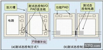
Figure 5: Two different test state control methods
For RFID, power consumption is an important issue in the chip design process. The series scheme is more efficient and more suitable for integrated circuit design. However, in terms of safety, the parallel scheme is a more ideal choice: the parallel connection of the power supply amplitude and ripple is controlled to the smallest possible range by the parallel bleeder circuit, so that the fluctuation of the power supply current consumption is suppressed after the rectifier circuit. Thus the AC signal across the antenna does not reflect the difference in state of any internal baseband system (mainly microprocessor).
2. Fault attack
A fault attack can cause one or more triggers to be ill, thereby corrupting the data transferred to registers and memory. Among the known non-destructive attacks on CPU smart cards, fault attacks are one of the most effective techniques in practical applications. There are currently three techniques that can reliably cause the trigger to be ill and affect very few machine cycles: transient clocks, transient power supplies, and transient external electric fields.
Clock failures can be implemented by simply increasing or decreasing the clock frequency for one or more half cycles so that some of the flip-flops sample their inputs before the legal new state arrives. Clock Failure Effective attacks are often combined with power failures. By combining clock and power fluctuations in contact smart cards, program counter content can be reliably increased without affecting other states of the processor. In this way, any sequence of instructions in the smart card can be executed by hackers, and the programmer does not have a good response in software writing.
Most RFID clocks and power supplies are obtained by using the AC signal shaping of the antenna. Therefore, clock-power failure attacks can be implemented by changing parameters such as the amplitude, symmetry, and frequency of the harmonics of the AC signal. With the help of digital direct synthesis of AC signal technology in RFID contact test equipment, it is easy to generate the waveforms required for clock-power failure attacks.
In order to effectively resist clock failure attacks, in addition to clock detectors, RFID products are more important to strictly limit the operating frequency range of RFID design, harmonic quality factors of carrier frequency, and symmetry. Therefore, from a security point of view, it is not the RFID that is more adaptable to the implement.
Potential failure techniques still need to be further explored, such as by applying a few hundred volts in a few milliseconds when the metal probe is placed at a processor's height of a few hundred microns, the resulting electric field strength is sufficient to change the nearby transistor threshold voltage. . The application value and countermeasures of these technologies have yet to be further studied.
RFID test status and protection
For the general sense of the integrated circuit industry chain, it is necessary to eliminate bad chips in the wafer testing stage to reduce unnecessary waste in the back-end processing, and RFID chips are no exception. According to the characteristics of the RFID chip, the wafer test content includes: RF performance test, logic function test and memory test. As with conventional chips, if on-chip logic and memory testing are performed with the help of chip application functions, the cost of testing will increase significantly. Equivalent test principles are often used to design additional test states for fast completion. Since the test state provides a fast, comprehensive access to the memory mechanism, it is necessary to permanently turn off the test state after the wafer test is completed.
Figure 5a shows the test state control method that has been widely used in the development of contact smart card chips: the additional I/O pins are connected to the internal circuit of the chip, and the wires pass through the dicing slots, so that the chips cannot pass after being cut. Simply control the pin to enter the test state. This approach is outdated due to the emergence of FIB patching technology. Figure 5b is the most promising alternative: designing partial control circuits in scribe slots and adjacent chips to obtain irreversible test state control.
Summary of this article
In this paper, the design of RFID chip is briefly discussed from three aspects: destructive, non-destructive attack and test state control. By comparing with the security design of contact smart card chip, some design measures are given. However, there are still many safety design measures that cannot be enumerated, such as current regulators and noise loads for power analysis. China's second-generation resident ID card is about to be implemented, which will be the largest RFID project in the world. It is of great practical significance to consider the security of its chip design.